1 浙江大学 光电科学与工程学院,极端光学技术与仪器全国重点实验室,浙江 杭州 310058
2 浙江大学 材料科学与工程学院,浙江 杭州 310058
随着人工智能、大数据、云计算、物联网、移动电子等的发展,传统的稀土离子掺杂单芯单模光纤放大器承载的光纤通信系统的传输容量已经逐渐接近香农极限,需要发展新型材料体系,以拓宽光纤通信系统的传输容量。相比于稀土离子,量子点具有较宽的发光带宽、可调波长的发光特性,且量子点的发光性质可以通过多种化学手段调控,在量子点光放大器上显示出了宽带光放大特性,受到学术界和产业界的广泛关注。在该背景下,本文提出将化学合成的PbS/CdS核壳量子点与低损耗聚合物集成,获得量子点掺杂光纤放大器,实现近红外通信波段可调波长、宽带光放大特性。文章研究并揭示了影响固化后的聚合物纤芯连续性的因素和影响机制,提出了降低固化胶前驱体液面附加压力、固化收缩力、聚合物前驱体与光纤内壁的摩擦力,并提高抽真空产生的牵引力以获得连续光纤,在此基础上获得了基于热固化聚二甲基硅氧烷(PDMS)和光固化NOA61、NOA85固化胶的纤芯连续光纤,量子点光纤在1 530~1 630 nm获得了增益带宽达到100 nm以上的开关增益,最高增益达到6.5 dB。本文的研究结果将促进量子点光纤器件和宽带光通信技术的发展。
量子点 聚合物光纤 宽带光纤放大器 quantum dots polymer optical fiber broadband optical fiber amplifier 
Author Affiliations
Abstract
The past two decades have seen a drastic progress in the development of semiconducting metal-halide perovskites (MHPs) from both the fundamentally scientific and technological points of view. The excellent optoelectronic properties and device performance make perovskites very attractive to the researchers in materials, physics, chemistry and so on. To fully explore the potential of perovskites in the applications, various techniques have been demonstrated to synthesize perovskites, modify their structures, and create patterns and devices. Among them, photo-processing has been revealed to be a facile and general technique to achieve these aims. In this review, we discuss the mechanisms of photo-processing of perovskites and summarize the recent progress in the photo-processing of perovskites for synthesis, patterning, ion exchange, phase transition, assembly, and ion migration and redistribution. The applications of photo-processed perovskites in photovoltaic devices, lasers, photodetectors, light-emitting diodes (LEDs), and optical data storage and encryption are also discussed. Finally, we provide an outlook on photo-processing of perovskites and propose the promising directions for future researches. This review is of significance to the researches and applications of perovskites and also to uncover new views on the light-matter interactions.The past two decades have seen a drastic progress in the development of semiconducting metal-halide perovskites (MHPs) from both the fundamentally scientific and technological points of view. The excellent optoelectronic properties and device performance make perovskites very attractive to the researchers in materials, physics, chemistry and so on. To fully explore the potential of perovskites in the applications, various techniques have been demonstrated to synthesize perovskites, modify their structures, and create patterns and devices. Among them, photo-processing has been revealed to be a facile and general technique to achieve these aims. In this review, we discuss the mechanisms of photo-processing of perovskites and summarize the recent progress in the photo-processing of perovskites for synthesis, patterning, ion exchange, phase transition, assembly, and ion migration and redistribution. The applications of photo-processed perovskites in photovoltaic devices, lasers, photodetectors, light-emitting diodes (LEDs), and optical data storage and encryption are also discussed. Finally, we provide an outlook on photo-processing of perovskites and propose the promising directions for future researches. This review is of significance to the researches and applications of perovskites and also to uncover new views on the light-matter interactions.
perovskites photo-processing optical properties opto-electronic devices Opto-Electronic Science
2022, 1(11): 220014
1 1.浙江大学 光电科学与工程学院, 杭州 310027
2 2.宁波匠心快速成型技术有限公司, 宁波 315000
传统“荧光粉+有机硅脂”荧光转换体的热导率低, 且物理化学稳定性差, 不能应用于高功率白光LED领域。全无机荧光块体材料可以规避有机封装, 具有更高的热导率, 但这类材料面临着成本高且极难实现立体结构的问题。本工作基于非晶态纳米二氧化硅, 得到一种包含(Gd,Y)AG:Ce荧光粉、可在紫外光下固化的浆料, 并通过光固化成型、空气排脂、无压烧结, 制备了一种(Gd,Y)AG:Ce荧光粉-石英玻璃复合材料。该荧光玻璃陶瓷在蓝光激发下发射峰值位于575 nm的宽带橙黄光, 且内量子效率大于90%。研究结果表明, 在致密化烧结过程中, (Gd,Y)AG:Ce荧光粉与石英玻璃之间的界面反应非常微弱, 因此荧光粉能够完好地嵌入到石英玻璃中。该全无机荧光转换体可以用于封装相关色温小于4500 K、显色指数大于75和流明效率为74 lm·W-1的高功率暖白光LED。所构建的激光照明器件的饱和激光功率密度可达2.84 W·mm-2, 此时光通量为180 lm。此外, 所提出的制备方法与3D打印兼容, 可以批量化制造出具有复杂立体结构的荧光转换体。该技术有望推动高功率白光LED朝着个性化和模块化发展。
荧光粉 玻璃陶瓷 暖白光 3D打印 glass-ceramics phosphors warm white light 3D printing 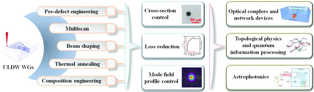
Author Affiliations
Abstract
1 Zhejiang University, College of Optical Science and Engineering, State Key Laboratory of Modern Optical Instrumentation, Hangzhou, China
2 Chinese Academy of Sciences, CAS Center for Excellence in Ultra-Intense Laser Science, Shanghai, China
Integrated photonics is attracting considerable attention and has found many applications in both classical and quantum optics, fulfilling the requirements for the ever-growing complexity in modern optical experiments and big data communication. Femtosecond (fs) laser direct writing (FLDW) is an acknowledged technique for producing waveguides (WGs) in transparent glass that have been used to construct complex integrated photonic devices. FLDW possesses unique features, such as three-dimensional fabrication geometry, rapid prototyping, and single step fabrication, which are important for integrated communication devices and quantum photonic and astrophotonic technologies. To fully take advantage of FLDW, considerable efforts have been made to produce WGs over a large depth with low propagation loss, coupling loss, bend loss, and highly symmetrical mode field. We summarize the improved techniques as well as the mechanisms for writing high-performance WGs with controllable morphology of cross-section, highly symmetrical mode field, low loss, and high processing uniformity and efficiency, and discuss the recent progress of WGs in photonic integrated devices for communication, topological physics, quantum information processing, and astrophotonics. Prospective challenges and future research directions in this field are also pointed out.
photonic integrated circuit waveguides femtosecond laser direct writing improved techniques photonic devices Advanced Photonics
2021, 3(2): 024002

Author Affiliations
Abstract
1 Nanjing University, College of Engineering and Applied Sciences, National Laboratory of Solid State Microstructures, Key Laboratory of Intelligent Optical Sensing and Integration, Jiangsu Key Laboratory of Artificial Functional Materials, Nanjing, China
2 Collaborative Innovation Center of Advanced Microstructures, Nanjing, China
3 Nanjing University, School of Electronic Science and Engineering, Nanjing, China
Metasurfaces have demonstrated unprecedented capabilities in manipulating light with ultrathin and flat architectures. Although great progress has been made in the metasurface designs and function demonstrations, most metalenses still only work as a substitution of conventional lenses in optical settings, whose integration advantage is rarely manifested. We propose a highly integrated imaging device with silicon metalenses directly mounted on a complementary metal oxide semiconductor image sensor, whose working distance is in hundreds of micrometers. The imaging performances including resolution, signal-to-noise ratio, and field of view (FOV) are investigated. Moreover, we develop a metalens array with polarization-multiplexed dual-phase design for a wide-field microscopic imaging. This approach remarkably expands the FOV without reducing the resolution, which promises a non-limited space-bandwidth product imaging for wide-field microscopy. As a result, we demonstrate a centimeter-scale prototype for microscopic imaging, showing uniqueness of meta-design for compact integration.
metalens compact imaging device polarization multiplexing wide-field microscopy Advanced Photonics
2020, 2(6): 066004
1 北京邮电大学信息光子学与光通信国家重点实验室, 北京 100876
2 北京邮电大学理学院, 北京 100876
设计了基于调制相移法的色散测量样机,提高了色散测量的精度,降低了色散测量成本。设计了基于幅相检测芯片AD8302的双鉴相电路,实现了相位差的准确测量。应用最小二乘法对接收的数据进行拟合,得到了可靠的色散系数曲线。整体采用模块化的设计思想,使用基于芯片F2812的数字信号处理,实现了对各模块插板的控制,完成了数据的采集和处理,并在实验室虚拟仪器工程工作台(LabVIEW)开发平台完成界面设计。对样机的性能进行了实验验证,结果表明,对于不同长度的G.652光纤,在波长1550 nm处,累积色散测量的不确定度小于10 ps/nm。
光通信 调制相移法 双鉴相电路 数字信号处理 最小二乘法 LabVIEW
1 中国科学院合肥物质科学研究院医学物理中心医用光谱质谱研究室, 安徽 合肥 230031
2 中国科学院安徽光学精密机械研究所, 安徽 合肥 230031
3 安徽农业大学, 安徽 合肥 230036
常温大气压下,在电子能量为0.35~0.65 eV的范围内,使用 氮气负电晕放电-电子吸附-离子迁移谱, 测量了CH2 Br2 , CH2 BrCl,CHBr3 的电子吸附速率常数,得到电子吸附速率常数的大小关系 为k(CH2 Br2 )>k(CH2 BrCl), k(CH2 Br2 )>k(CHBr3 ),并根据电子亲和势对CH2 Br2 和CH2 BrCl的 大小关系进行理论分析。首次对CHBr3 的电子吸附过程进行了定性分析,发现样品蒸汽 在迁移区通入迁移管时,溴离子会与CHBr3 分子络合成团簇离子Br-(H2 O)n (CHBr3 )m 。
光谱学 离子迁移谱 电晕放电 速率常数 spectroscopy ion mobility spectrometry corona discharge rate constant


